New device could greatly improve speech and image recognition

150511172759_1_540x360

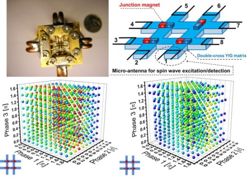
Clockwise, photo of the prototype device; schematic of the eight-terminal magnonic holographic memory prototype; collection of experimental data obtained for two magnonic matrixes.

Researchers at the University of California, Riverside Bourns College of Engineering and the Russian Academy of Sciences have successfully demonstrated pattern recognition using a magnonic holographic memory device, a development that could greatly improve speech and image recognition hardware.

Pattern recognition focuses on finding patterns and regularities in data. The uniqueness of the demonstrated work is that the input patterns are encoded into the phases of the input spin waves.

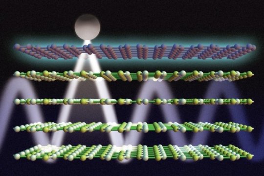
Spin waves are collective oscillations of spins in magnetic materials. Spin wave devices are advantageous over their optical counterparts because they are more scalable due to a shorter wavelength. Also, spin wave devices are compatible with conventional electronic devices and can be integrated within a chip.

The researchers built a prototype eight-terminal device consisting of a magnetic matrix with micro-antennas to excite and detect the spin waves. Experimental data they collected for several magnonic matrixes show unique output signatures correspond to specific phase patterns. The microantennas allow the researchers to generate and recognize any input phase pattern, a big advantage over existing practices.

Then spin waves propagate through the magnetic matrix and interfere. Some of the input phase patterns produce high output voltage, and other combinations results in a low output voltage, where “high” and “low” are defined regarding the reference voltage (i.e. output is high if the output voltage is higher than 1 millivolt, and low if the voltage is less than 1 millivolt.

It takes about 100 nanoseconds for recognition, which is the time required for spin waves to propagate and to create the interference pattern.

The most appealing property of this approach is that all of the input ports operate in parallel. It takes the same amount of time to recognize patterns (numbers) from 0 to 999, and from 0 to 10,000,000. Potentially, magnonic holographic devices can be fundamentally more efficient than conventional digital circuits.

The work builds upon findings published last year by the researchers, who showed a 2-bit magnonic holographic memory device can recognize the internal magnetic memory states via spin wave superposition. That work was recognized as a top 10 physics breakthrough by Physics World magazine.

“We were excited by that recognition, but the latest research takes this to a new level,” said Alex Khitun, a research professor at UC Riverside, who is the lead researcher on the project. “Now, the device works not only as a memory but also a logic element.”

The latest findings were published in a paper called “Pattern recognition with magnonic holographic memory device” in the journal Applied Physics Letters. In addition to Khitun, authors are Frederick Gertz, a graduate student who works with Khitun at UC Riverside, and A. Kozhevnikov, Y. Filimonov and G. Dudko, all from the Russian Academy of Sciences.

Holography is a technique based on the wave nature of light which allows the use of wave interference between the object beam and the coherent background. It is commonly associated with images being made from light, such as on driver’s licenses or paper currency. However, this is only a narrow field of holography.

Holography has been also recognized as a future data storing technology with unprecedented data storage capacity and ability to write and read a large number of data in a highly parallel manner.

The main challenge associated with magnonic holographic memory is the scaling of the operational wavelength, which requires the development of sub-micrometer scale elements for spin wave generation and detection.

References:http://www.sciencedaily.com/

Controlling light: Scientists tune light waves by pairing exotic 2-D materials

150520100607_1_540x360

Researchers have shown that a DC voltage applied to layers of graphene and boron nitride can be used to control light emission from a nearby atom. Here, graphene is represented by a maroon-colored top layer; boron nitride is represented by yellow-green lattices below the graphene; and the atom is represented by a grey circle. A low concentration of DC voltage (in blue) allows the light to propagate inside the boron nitride, forming a tightly confined waveguide for optical signals. Researchers have shown that a DC voltage applied to layers of graphene and boron nitride can be used to control light emission from a nearby atom. Here, graphene is represented by a maroon-colored top layer; boron nitride is represented by yellow-green lattices below the graphene; and the atom is represented by a grey circle. A low concentration of DC voltage (in blue) allows the light to propagate inside the boron nitride, forming a tightly confined waveguide for optical signals.

Researchers have found a way to couple the properties of different two-dimensional materials to provide an exceptional degree of control over light waves. They say this has the potential to lead to new kinds of light detection, thermal-management systems, and high-resolution imaging devices.

The new findings — using a layer of one-atom-thick graphene deposited on top of a similar 2-D layer of a material called hexagonal boron nitride (hBN) — are published in the journal Nano Letters. The work is co-authored by MIT associate professor of mechanical engineering Nicholas Fang and graduate student Anshuman Kumar, and their co-authors at IBM’s T.J. Watson Research Center, Hong Kong Polytechnic University, and the University of Minnesota.

Although the two materials are structurally similar — both composed of hexagonal arrays of atoms that form two-dimensional sheets — they each interact with light quite differently. But the researchers found that these interactions can be complementary, and can couple in ways that afford a great deal of control over the behavior of light.

The hybrid material blocks light when a particular voltage is applied to the graphene, while allowing a special kind of emission and propagation, called “hyperbolicity,” when a different voltage is applied — a phenomenon not seen before in optical systems, Fang says. One of the consequences of this unusual behavior is that an extremely thin sheet of material can interact strongly with light, allowing beams to be guided, funneled, and controlled by voltages applied to the sheet.

“This poses a new opportunity to send and receive light over a very confined space,” Fang says, and could lead to “unique optical material that has great potential for optical interconnects.” Many researchers see improved interconnection of optical and electronic components as a path to more efficient computation and imaging systems.

Light’s interaction with graphene produces particles called plasmons, while light interacting with hBN produces phonons. Fang and his colleagues found that when the materials are combined in a certain way, the plasmons and phonons can couple, producing a strong resonance.

The properties of the graphene allow precise control over light, while hBN provides very strong confinement and guidance of the light. Combining the two makes it possible to create new “metamaterials” that marry the advantages of both, the researchers say.

Phaedon Avouris, a researcher at IBM and co-author of the paper, says, “The combination of these two materials provides a unique system that allows the manipulation of optical processes.”

The combined materials create a tuned system that can be adjusted to allow light only of certain specific wavelengths or directions to propagate, they say. “We can start to selectively pick some frequencies [to let through], and reject some,” Kumar says.

These properties should make it possible, Fang says, to create tiny optical waveguides, about 20 nanometers in size — the same size range as the smallest features that can now be produced in microchips. This could lead to chips that combine optical and electronic components in a single device, with far lower losses than when such devices are made separately and then interconnected, they say.

Co-author Tony Low, a researcher at IBM and the University of Minnesota, says, “Our work paves the way for using 2-D material heterostructures for engineering new optical properties on demand.”

Another potential application, Fang says, comes from the ability to switch a light beam on and off at the material’s surface; because the material naturally works at near-infrared wavelengths, this could enable new avenues for infrared spectroscopy, he says. “It could even enable single-molecule resolution,” Fang says, of biomolecules placed on the hybrid material’s surface.

Sheng Shen, an assistant professor of mechanical engineering at Carnegie Mellon University who was not involved in this research, says, “This work represents significant progress on understanding tunable interactions of light in graphene-hBN.” The work is “pretty critical” for providing the understanding needed to develop optoelectronic or photonic devices based on graphene and hBN, he says, and “could provide direct theoretical guidance on designing such types of devices. … I am personally very excited about this novel theoretical work.”

The research team also included Kin Hung Fung of Hong Kong Polytechnic University. The work was supported by the National Science Foundation and the Air Force Office of Scientific Research.

References:http://www.sciencedaily.com/

Mobile input device Phree invites you to jot, sketch, take notes

mobileinputd.jpg1

A Kickstarter campaign is heating up over a device called Phree. It’s for writing on nearly any surface you want to and seeing your writing instantly appear on your screen. In a promotional video, a presenter says, “In 2015 we love our touchscreeens.” Only, there’s one problem: “They are not a perfect input device.” Users need better precision and more space, and so Phree was created, taking you way beyond the screen.

This is a high-resolution mobile input device, where you can sketch or jot down notes, thoughts, addresses, numbers, and such, without the added effort of having to unlock a phone, open an app and wait.
Phree will connect to a range of devices: phone, tablet, laptop, TV, anything with a Bluetooth connection. They said Phree is compatible with Office, OneNote, EverNote, Acrobat, and more. Also, they said Phree supports all major phone, tablet and PC operating systems – Android, iOS, Windows, OSX, Linux.
Opher Kinrot, Uri Kinrot, chief engineer and Gilad Lederer are co-founders of the Tel Aviv-based company OTM Technologies, which created Phree. Elisha Tal is the chief designer.
The design involves an oval cross-section for usefulness and comfort. Held in writing position, Phree’s touch display always faces the user. One can touch to change from pen to highlighter or from red to blue or from messaging to dialing. Phree prototypes are in black, graphite, silver and gold.
They have turned to Kickstarter to push Phree closer to market and delivery stages.
The key driver that enables Phree is “Optical Translation Measurement” (OTM) technology, which precisely tracks hand motion across a surface. They have engineered and built a compact optical sensor that fits at the tip of a pen-like device.

The OTM sensor is a 3D laser interferometer. It tracks the relative motion of a nearby surface, they said, by measuring the interference signal between a laser beam projected on the surface and reflections from the surface. The signal is translated to X-Y-Z motion information by their signal-processing algorithms running on a small, integrated electronics component

.1-mobileinputd.jpg2

The battery will last around one week for typical usage. Full charging time is about one hour.
For developers, the good news is that this is an open platform. They said, “An open API allows developers to make use of the screen for specific interaction with their applications. The API provides access to additional sensor information such as vertical (Z) motion data, as well as access to the accelerometer.”
The Kickstarter page lists the range of prices and reward details. At the time of this writing, for example, a pledge of $316 would bring a twin pack of two Phree devices A pledge of $219 would get one Phree and case. Estimated delivery date for both price offers is April 2016

References:http://phys.org/


New printing process makes three-dimensional objects glow

newprintingp

Conventional electroluminescent (EL) foils can be bent up to a certain degree only and can be applied easily onto flat surfaces. The new process developed by Karlsruhe Institute of Technology (KIT) in cooperation with the company of Franz Binder GmbH & Co. now allows for the direct printing of electroluminescent layers onto three-dimensional components. Such EL components might be used to enhance safety in buildings in case of power failures. Other potential applications are displays and watches or the creative design of rooms.

“By means of the innovative production process we developed together with our industry partner, any type of three-dimensional object can be provided with electroluminescent coatings at low costs,” Dr.-Ing. Rainer Kling of the Light Technology Institute of KIT says. Usually, the luminescent material is located between two plastic layers in EL carrier foils. By means of the new printing process, however, the electroluminescent layers are directly printed onto the object without any intermediate carrier. In this way, convex and concave surfaces of various materials, such as paper or plastic, can be made glow.
The different components of the coating, including the electroluminescent and the electrically conductive materials, are applied by a novel pad printing process. The pad printing machine is equipped with an elastic rubber pad that is easily deformable and, hence, excellently suited for the coating of curved surfaces.
“In this way, it is possible to provide surfaces and even spheres with homogeneous coatings at low costs,” says engineer Elodie Chardin, who works on this research project. “Homogeneity of the coating of about one tenth of a millimeter in thickness was one of the challenges of this project,” says the executive engineer of the industry partner, Elisabeth Warsitz. The process requires a few production steps only and, hence, is characterized by a low consumption of resources. By using various luminescent substances, various colors may be applied to the same surface.

The research and development project of KIT in cooperation with the Binder Connector Group, headquartered in the German town of Neckarsulm, took about two years and was funded with EUR 125,000 by the Deutsche Bundesstiftung Umwelt (German Foundation for the Environment).

References:http://phys.org/